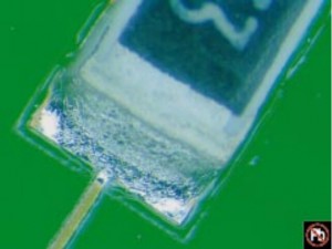
Acceptability for Electronic Assemblies :Soldering Acceptability Requirements
Target-Class1,2,3
.Solder fillet appears generally smooth and exhibits good wetting of the solder to the parts being joined.
.Outline of the parts is easily determined.
.Solder at the part being joined creates a feathered edge.
.Fillet is concave in shape.
See pic for examples of soldering anomalies.
Acceptable-Class1,2,3
.There are materials and processes,e.g.,lead free alloys and slow cooling with large mass PCBs, that may produce dull
matte,gray,or grainy appearing solders that are normal for the material or process involved.These solder connections
are acceptable.
.The solder connection wetting angle (solder to component and solder to PCB termination do not exceed 90°(Figure).
.As an exception,the solder connection to a termination may exhibit a wetting angle exceeding 90°(Figure)when it is
created by the solder contour extending over the edge of the solder able termination area or solder resist.
Figures below illustrate acceptable solder connections with various solder alloys and process conditions.
SnPb Solder; No Clean Process SnAgCu Solder;No Clean Process
SnPb Solder;Water Soluble Flux SnAgCu Solder;Water Soluble Flux
SnPb Solder; Water Soluble Flux SnAgCu Solder;Water Soluble Flux
SnAgCu Solder;No Clean Process,N2 Reflow SnAgCu Solder,No Clean Process;Air Reflow
SnPb Solder;No Clean Process SnAgCu Solder;No Clean Process
SnPb Solder;No Clean Process SnAgCu Solder;No Clean Process
SnPb Solder SnAgCu Solder
SnPb Solder SnAgCu Solder
SnPb Solder ; OSP Finish SnAgCu Solder; OSP Finish
SnAg CuSolder SnAg CuSolder
SnAgCu Solder SnAgCu Solder
Soldering Anomalies-Exposed Basis Metal
Exposed basis metal on component leads,conductors or land surfaces from nicks,scratches,or other conditions cannot exceed
there quirements of 7.1.2.3 for leads and 10.2.9.1 for conductors and lands.
Component leads,sides of land patterns,conductors,and use of liquid photo image able solder resist,can have exposed basis
metal per original designs.
Some printed circuit board and conductor finishes have different wetting characteristics and may exhibit solder wetting only to
specific areas. Exposed basis metal or surface finishes should be considered normal under these circumstances,provided the
achieved wetting characteristics of the solder connection areas are acceptable.
Acceptable-Class 1,2,3
.Exposed basis metal on:
.Vertical conductor edges.
.Cut ends of component leads or wires.
.Organic Solderability Preservative (OSP) coated lands.
.Exposed surface finishes that are not part of the required solder fillet area.
Acceptable-Class 1
Process Indicator-Class 2,3
.Exposed basis metal on component leads,conductors or land surfaces from nicks or scratches provided conditions
do not exceed the requirements of7.1.2.3 for leads and 10.2.9.1 for conductors and lands.
Soldering Anomalies-Pin Holes/Blow Holes
Acceptable-Class1
ProcessIndicator-Class2,3
.Blowholes (Figures 1,2),pinholes (Figure 3),voids (Figures 4,5),etc.,providing the solder connection meets all other requirements.
1 2


3 4
5
Defect-Class 2,3
Solder connections where pin holes,blowholes,voids,etc.
reduce the connections below minimum requirements(not shown).
Soldering Anomalies-Reflow of Solder Paste
Defect-Class1,2,3
.Incomplete reflow of solder paste.

Soldering Anomalies-Nonwetting
IPC-T-50 defines nonwetting as the inability of molten solder to form a metallic bond with the basis metal.In this Standard,that
includes surface finishes.
Defect-Class 1,2,3
.Solder has not wetted to the land or termination where solder is required.
.Solder coverage does not meet requirements for this termination type.
Soldering Anomalies-Dewetting
Defect-Class 1,2,3
.Evidence of dewetting that causes the solder connection to not meet the SMT and thru-hole solder fillet requirements.
Soldering Anomalies-Excess Solder-Solder Balls/Solder Fines
Solder balls are spheres of solder that remain after the soldering process.Solder fines are typically small balls of the original
solder paste metal screen size that have splattered around the connection during there flow process.
Target-Class 1,2, 3
.No evidence of solder balls on the printed wiring assembly.
Acceptable-Class 1,2,3
.Solder balls are entrapped/encapsulated and do not violate minimum electrical clearance.
Note:Entrapped/encapsulated/attached is intended to mean that normal service environment of the product will not cause a solder ball to become dislodged.
Defect- Class 1,2,3
.Solder balls violate minimum electrical clearance.
.Solder balls are not entrapped in no-clean residue or encapsulated with conformal coating,
or not attached(soldered)to a metal surface.
Soldering Anomalies-Excess Solder-Bridging
Defect-Class 1,2,3
.A solder connection across conductors that should not be joined.
.Solder has bridged to adjacent noncommon conductoror component.
Soldering Anomalies-Excess Solder-Solder Webbing/Splashes
Defect-Class 1,2,3
.Solder splashes/webbing.
Soldering Anomalies-Disturbed Solder
Surface appearance with cooling lines as shown in Acceptable pic is more likely to occur in lead free alloys and is not a disturbed solder condition.
Defect-Class 1,2,3
Characterized by stress lines from movement in the connection (SnPb alloy).
Soldering Anomalies-Fractured Solder
Defect-Class 1,2,3
Fractured or cracked solder.
Soldering Anomalies-Solder Projections
Defect-Class 1,2,3
.Solder projection,figure 1,violates assembly maximum
height requirements or lead protrusion requirements.
.Projection,figure 2,violates minimum electrical clearance(1).
1 2
Soldering Anomalies-Lead Free Fillet Lift
Acceptable-Class 1,2.3
.Fillet lifting-separation of the bottom of the solder and the
top of the land(primary side of plated-through hold connection).
Process Indicator-Class 2
Defect-Class3
.Fillet lifting-separation of the bottom of the solder and the top of the land(secondary side of plated-through hold connection)(not shown).
Defect-Class 1,2,3
.Fillet lifting damages the land attachment.
Soldering Anomalies-Hot Tear/Shrink Hole
Acceptable-Class1,2,3
.For connections made with lead free alloys:
.The bottom of the tear is visible.
.The tear or shrink hole does not contact the lead,land or
barrel wall.
Defect-Class 1,2,3
.Shrink holes or hot tear in connections made with SnPb solder alloys:
.For connections made with lead free alloys:
.The bottom of the shrink hole or hot tear is not visible.
.The tear or shrink hole contacts the lead or land.
end


